| infotek | 2024-09-04 07:52 |
OptiFDTD应用:光栅衍射的远场分布•使用VB脚本生成光栅(或周期性)布局。 •光栅布局模拟和后处理分析 布局layout 我们将模拟如图1所示的二维光栅布局。 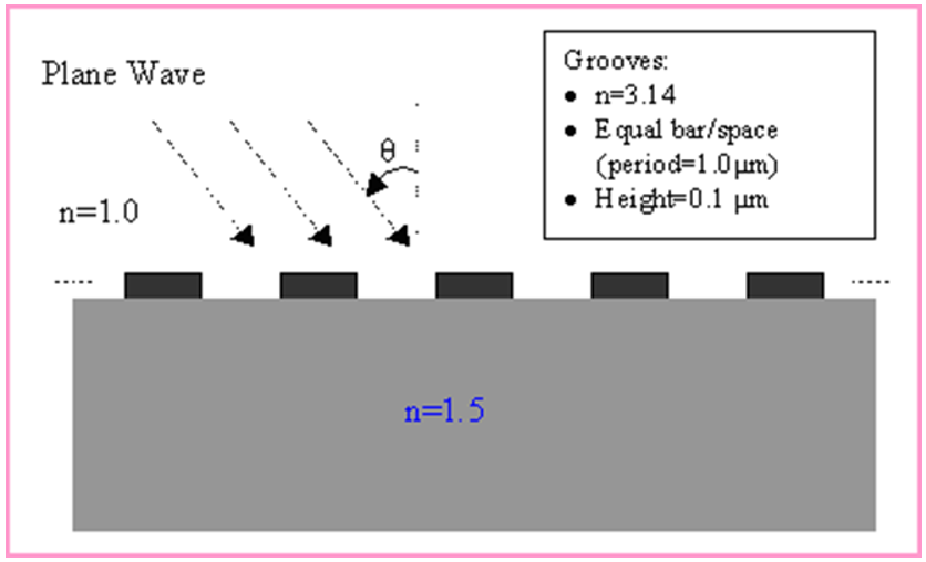 图1.二维光栅布局 用VB脚本定义一个2D光栅布局 步骤: 1 通过在文件菜单中选择“New”,启动一个新项目。 2 在“Wafer Properties”对话框中设置以下参数 Wafer Dimensions: Length (mm): 8.5 Width (mm): 3.0 2D wafer properties: Wafer refractive index: Air 3 点击 Profiles 与 Materials. 在“Materials”中加入以下材料: Name: N=1.5 Refractive index (Re:): 1.5 Name: N=3.14 Refractive index (Re:): 3.14 4.在“Profile”中定义以下轮廓: Name: ChannelPro_n=3.14 2D profile definition, Material: n=3.14 Name: ChannelPro_n=1.5 2D profile definition, Material: n=1.5 6.画出以下波导结构: a. Linear waveguide 1 Label: linear1 Start Horizontal offset: 0.0 Start vertical offset: -0.75 End Horizontal offset: 8.5 End vertical offset: -0.75 Channel Thickness Tapering: Use Default Width: 1.5 Depth: 0.0 Profile: ChannelPro_n=1.5 b. Linear waveguide 2 Label: linear2 Start Horizontal offset: 0.5 Start vertical offset: 0.05 End Horizontal offset: 1.0 End vertical offset: 0.05 Channel Thickness Tapering: Use Default Width: 0.1 Depth: 0.0 Profile: ChannelPro_n=3.14 7.加入水平平面波: Continuous Wave Wavelength: 0.63 General: Input field Transverse: Rectangular X Position: 0.5 Direction: Negative Direction Label: InputPlane1 2D Transverse: Center Position: 4.5 Half width: 5.0 Titlitng Angle: 45 Effective Refractive Index: Local Amplitude: 1.0  图2.波导结构(未设置周期) 8.单击“Layout Script”快捷工具栏或选择仿真菜单下的“Generate Layout Script…”。这一步将把布局对象转换为VB脚本代码。 将Linear2代码段修改如下: Dim Linear2 for m=1 to 8 Set Linear2 = WGMgr.CreateObj ( "WGLinear", "Linear2"+Cstr(m) ) Linear2.SetPosition 0.5+(m-1)*1.0, 0.05, 1+(m-1)*1.0, 0.05 Linear2.SetAttr "WidthExpr", "0.1" Linear2.SetAttr "Depth", "0" Linear2.SetAttr "StartThickness", "0.000000" Linear2.SetAttr "EndThickness", "0.000000" Linear2.SetProfileName "ChannelPro_n=3.14" Linear2.SetDefaultThicknessTaperMode True 点击“Test Script”快捷工具栏运行修改后的VB脚本代码。生成光栅布局,布局如图3所示。 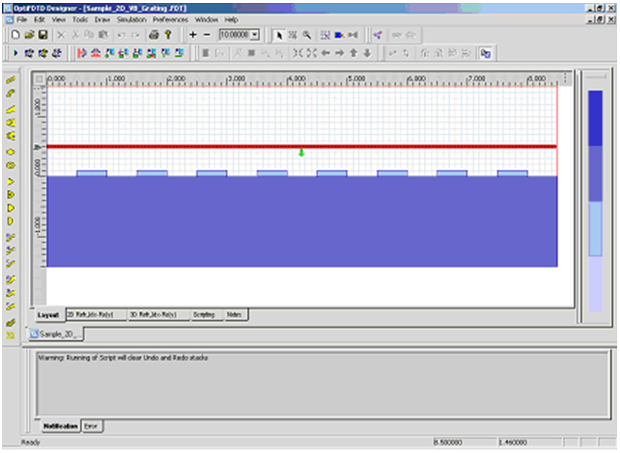 图3.光栅布局通过VB脚本生成 设置仿真参数 1. 在Simulation菜单下选择“2D simulation parameters…”,将出现仿真参数对话框 2. 在仿真参数对话框中,设置以下参数: TE simulation Mesh Delta X: 0.015 Mesh Delta Z: 0.015 Time Step Size: Auto Run for 1000 Time steps 设置边界条件设置X和Z边为各向异性PML边界条件。 Number of Anisotropic PML layers: 15 其它参数保持默认 运行仿真 • 在仿真参数中点击Run按钮,启动仿真 • 在分析仪中,可以观察到各场分量的时域响应 • 仿真完成后,点击“Yes”,启动分析仪。 远场分析衍射波 1. 在OptiFDTD Analyzer中,在工具窗口中选择“Crosscut Viewer” 2. 选择“Definition of the Cross Cut”为z方向 3. 将位置移动到等于92的网格点,(位置:-0.12)观察当前位置的近场 4. 在Crosscut Viewer的工具菜单中选择“Far Field”,出现远场转换对话框。(图4) 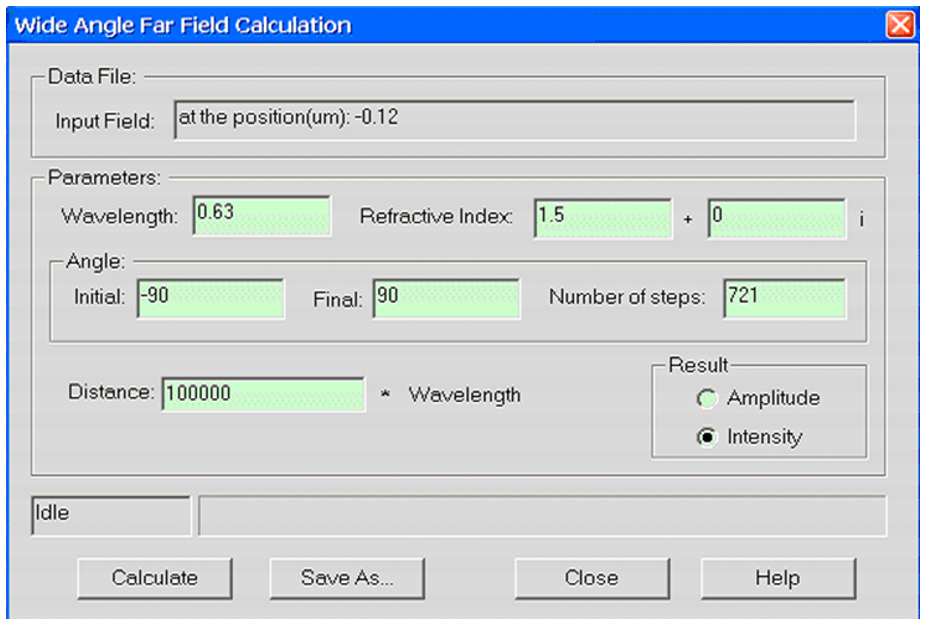 图4.远场计算对话框 5. 在远场对话框,设置以下参数: Wavelength: 0.63 Refractive index: 1.5+0i Angle Initial: -90.0 Angle Final: 90.0 Number of Steps: 721 Distance: 100, 000*wavelength Intensity 6. 点击“计算”按钮开始计算,并将结果保存为 Farfield.ffp。 7. 启动“Opti 2D Viewer”并加载Farfield.ffp。远场如图5所示。 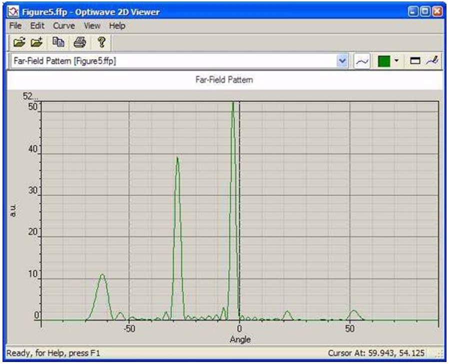 图5.“Opti 2D Viewer”中的远场模式
|
|